
")
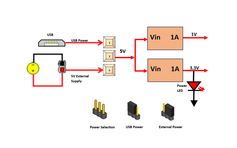
TheSPARTAN6STARTER KITcan work on USB power you can also connect external 5VDc. supply. When JP2 jumper is placed in 2 & 3 power is used from USB connector. When JP2jumper is placed in 1&2 power is used from external power adaptor
Use external 5V/2A supply whenever you are using steeper or dc motor.
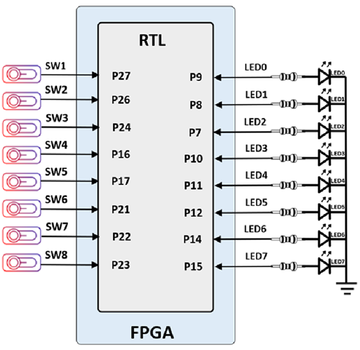
TheSPARTAN6STARTER KIT+board has 8 individual LED & 8 slide switches.A LED is assigned to each I/O to indicate its data status when I/O is configured as output. DIP switch is used to provide digital input (i.e. logic 0 and logic 1).
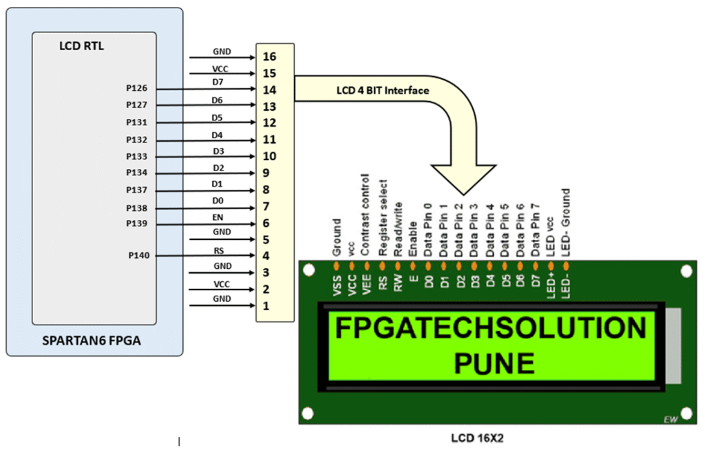
The SPARTAN6 STARTER KIT includes 2 lines by 16 characters LCD (liquid crystal display) Module. The dot matrix LCD displays alphanumeric characters, numbers and symbols. For displaying characters, numbers and symbol, user needs to send 8-bit ASCII value on data pins (Data0-Data8). The user can control the LCD display by controlling control lines (RS, EN) and sending command codes on data pins. All the functions required for controlling LCD backlight are provided internally on board. Internal refresh is provided by the controller. The Interface details of the LCD display are as shown in following figure
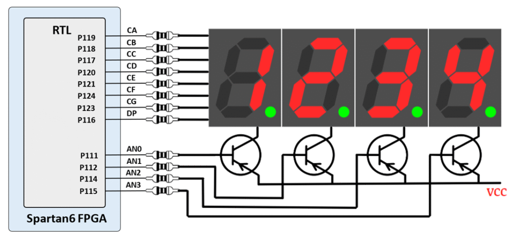
The SPARTAN6 STARTER KIT board contains a four-digit common anode seven-segment LED display. Each of the four digits is composed of seven segments arranged in a “figure 8” pattern, with an LED embedded in each segment. Segment LEDs can be individually illuminated, so any one of 128 patterns can be displayed on a digit by illuminating certain LED segments and leaving the others dark. Of these 128 possible patterns, the ten corresponding to the decimal digits are the most useful.
The anodes of the seven LEDs forming each digit are tied together into one “common anode” circuit node, but the LED cathodes remain separate. The common anode signals are available as four “digit enable” input signals to the 4-digit display. The cathodes of similar segments on all four displays are connected into seven circuit nodes labeled CA through CG (so, for example, the four “D” cathodes from the four digits are grouped together into a single circuit node called “CD”). These seven cathode signals are available as inputs to the 4-digit display. This signal connection scheme creates a multiplexed display, where the cathode signals are common to all digits but they can only illuminate the segments of the digit whose corresponding anode signal is asserted.
The SPARTAN6 STARTER KIT board includes anADC MCP3004. The ADC has 4 analog input channels. The channels are selected by setting the address pins of ADC. The analog input to all channels is given by external circuit through relimate pins. The other controlling signals of ADC are interfaced with FPGA board as shown in following figure. VREF is connected to 3.3V, so analog voltage input rang of all channel is 0 to 3.3V.
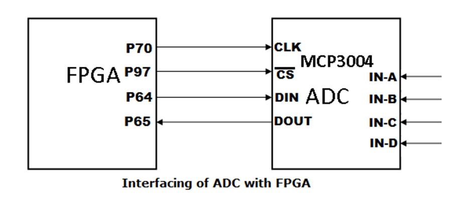
Pin assignment (UCF Location) for ADC:
| Signal Name | XC6SLX9 |
|---|---|
| CLK | P70 |
| CS | P97 |
| DIN | P65 |
| DOUT | P64 |
The SPARTAN6 STARTER KIT board includes 8-bit 4 channels, digital-to-analog converter (DACs)DAC084S085. DAC allows easy interface to most popular microprocessor buses and output ports. DAC works on 3.3V. The following figure shows the interfacing diagram of DAC with FPGA Board.VREF is connected to 3.3V, so analog voltage output rang of all channel is 0 to 3.3V.
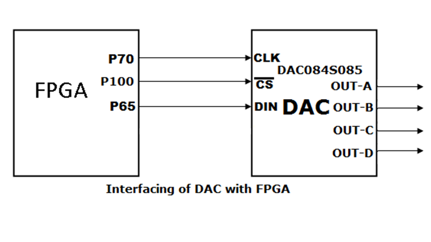
| Signal Name | XC6SLX9 |
|---|---|
| CS | P100 |
| CLK | P70 |
| DIN | P65 |
http://www.ftdichip.com/Support/Documents/DataSheets/ICs/DS_FT2232H.pdf USB-UART bridge (attached to connector J6) that allows you to use PC applications to communicate with the board using standard Windows COM port commands. Free USB-COM port drivers, available from www.ftdichip.com under the “Virtual Com Port” or VCP heading, convert USB packets to UART/serial port data. Serial port data is exchanged with the FPGA using a two-wire serial port (TXD/RXD). After the drivers are installed, I/O commands can be used from the PC directed to the COM port to produce serial data traffic on the M5 and L5 FPGA pins.
The FT2232HL is also used as the controller for the USB-JTAG circuitry, but the USB-UART and USB-JTAG functions behave entirely independent of one another. Programmers interested in using the UART functionality of the FT2232 within their design do not need to worry about the JTAG circuitry interfering with the UART data transfers, and vice-versa. The combination of these two features into a single device allows the PINE-S7 to be programmed, communicated with via UART, and powered from a computer attached with a single Micro USB cable. The connections between the FT2232HQ and the Artix-7 are shown in the below figure.
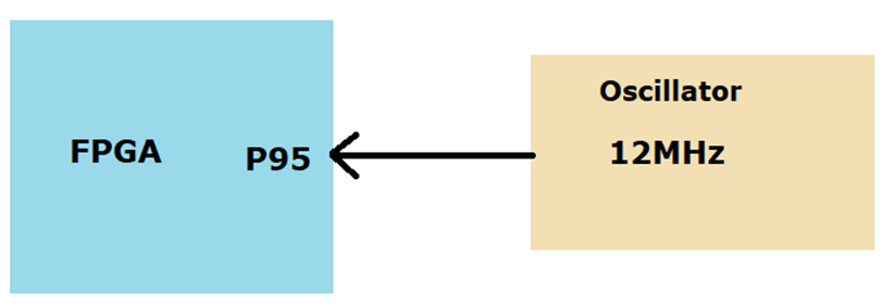
The SPARTAN6 STARTER KITsupports clock input sources which shown below fig. The board includes an on-board 12 MHz clock oscillator
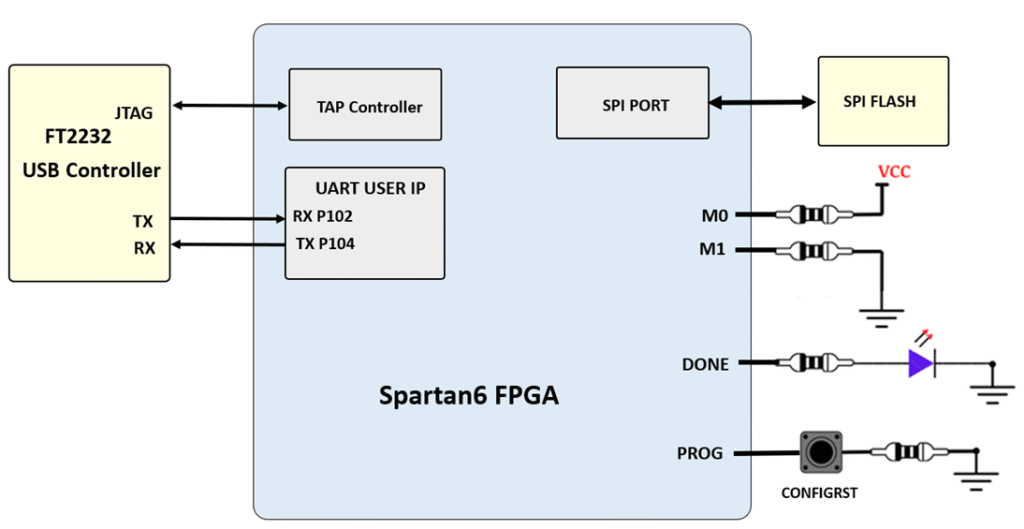
The SPARTAN6 STARTER KIT board contains a8Mbit non-volatile serial Flash device, which is attached to the Spartan 6 FPGA using SPI bus. The connections and pin assignments between the FPGA and the serial flash device are shown the below figure
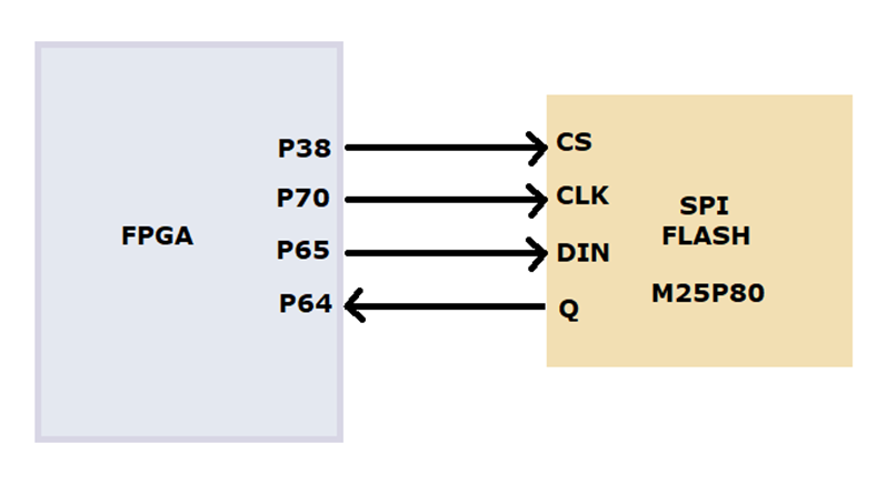
Board have been loaded with a Flash device (part number M25P80).FPGA configuration files can be written to the SPI Flash, and mode settings are available to cause the FPGA to automatically read a configuration from this device at power on. An FPGA configuration file requires just over one Mbytes of memory, leaving approximately 50% of the flash device available for user data.
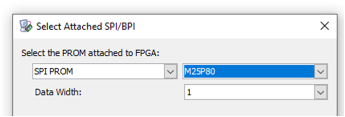
Select following flash while programming mcs file
On this board you can control either steeper motor or Dc motor at a time
Use external 5V/2A supply whenever you are using steeper or dc motor.
Connect steeper motor as shown in following fig
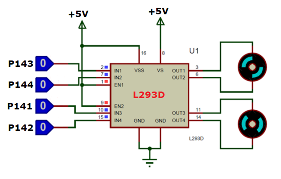
In order to have a complete control over DC motor, we have to control its speed and rotation direction. This can be achieved by combining these two techniques.PWM – For controlling spee,H-Bridge – For controlling rotation direction This both can be achieved by L293D motor driver IC
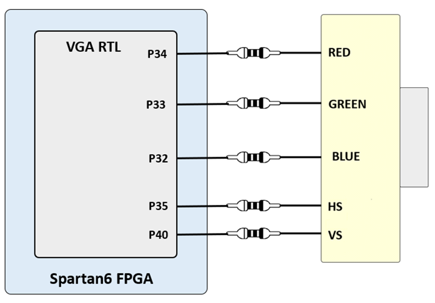
The SPARTAN6 STARTER KIT board uses 5 FPGA signals to create a VGA port with 1 bits-per-color and the two standard sync signals (HS – Horizontal Sync, and VS – Vertical Sync). The color signals use resistor-divider circuits that work in conjunction with the 82-ohm termination resistance of the VGA display to create 16 signal levels each on the red, green, and blue VGA signals.
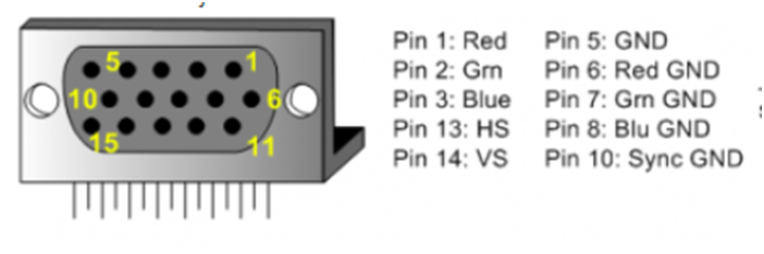
This circuit, shown in the above diagram, , produces video color signals that proceed in equal increments between 0V (fully off) and 0.7V (fully on). Using this circuit, 4096 different colors can be displayed, one for each unique 3-bit pattern. A video controller circuit must be created in the FPGA to drive the sync and color signals with the correct timing in order to produce a working display system.
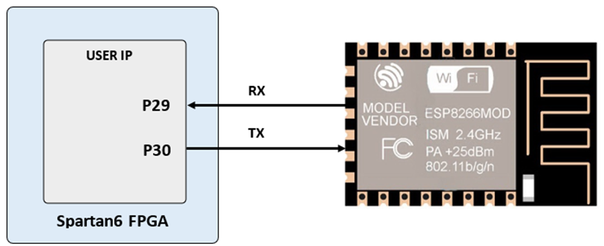
Very popular ESP12-F module is connected with FPGA on board shown bellow, using this many IOT application can be done, few example source code are give along with kit
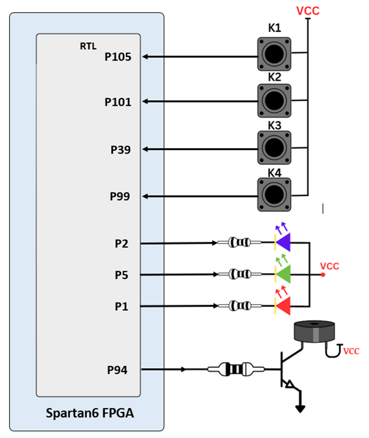
Spartan6 starter kithave four push button, RGB LED & buzzer connected with FPGA shown as below, this can be used various different purposes
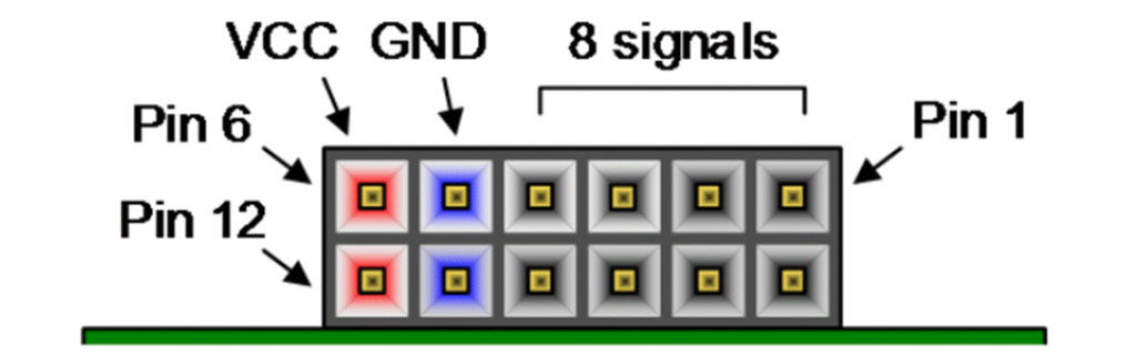
We have a large collection of Pmod (Peripheral Module) accessory boards that can attach to the expansion ports to add ready-made functions such as A/D’s, D/A’s, motor drivers, sensors, displays, and many other functions. These ports can be used as simple expansion ports, since all of the pin-outs correspond to pins on the FPGA.
The Pmod ports are arranged in a 2×6 right-angle, and are 100-mil female connectors that mate with standard 2×6 pin headers. Each 12-pin Pmod ports provides two 3.3V VCC signals (pins 6 and 12), two Ground signals (pins 5 and 11), and eight logic signals. The VCC and Ground pins can deliver up to 1A of current. Pmod data signals are not matched pairs, and they are routed using best-available tracks without impedance control or delay matching. Pin assignments for the Pmod I/O connected to the FPGA are shown in the below table
Warning: Since the Pmod pins are connected to Spartan-6 FPGA pins using a 3.3V logic standard, care should be taken not to drive these pins over 3.4V.
| Pmod JA | Pmod JB | Pmod JC | Pmod JD |
|---|---|---|---|
| JA1 :P48 | JB1 :P61 | JC1 :P81 | JD1 :P93S |
| JA2 :P46 | JB2 :P58 | JC2 :P79 | JD2 :P88 |
| JA3 :P44 | JB3 :P56 | JC3 :P75 | JD3 :P85 |
| JA4 :P41 | JB4 :P51 | JC4 :P67 | JD4 :P83 |
| JA7 :P50 | JB7 :P62 | JC7 :P80 | JD7 :P92 |
| JA8 :P47 | JB8 :P59 | JC8 :P78 | JD8 :P87 |
| JA9 :P45 | JB9 :P57 | JC9 :P74 | JD9 :P84 |
| JA10 :P43 | JB10 :P55 | JC10:P66 | JD10:P82 |
Table of Contents
Toggle