
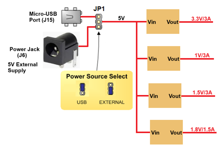
The EISLER ARTIX7 FPGA BOARD ARTIX7 FPGA A7uses +5V power supply to function properly. By default theboard is configured to use +5V supply from USB. So an external +5Vpower is not required unless USB port is unable to supply enoughcurrent. In most cases USB ports are capable of providing enoughcurrent for the module. Current requirement for this board largelydepends on your application. Please consult FPGA data sheet for moredetails on power requirements. If for any reason, an external 5V powersupply needs to be used for the module, the Power select jumper shouldbe configured properly as shown below When JP1 jumper is placed towards USB as shown in below image power is used from USB connector & when JP1 jumper is placed towards power connector power is used from external connector
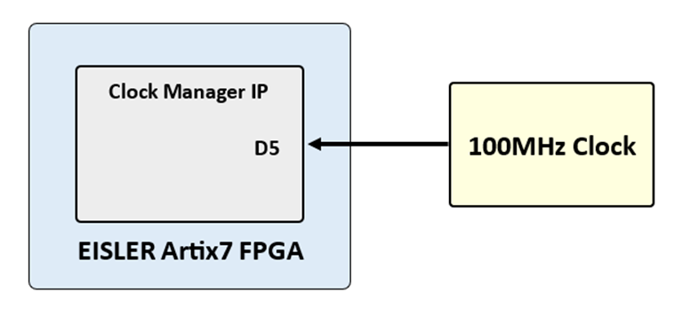
The EISLER ARTIX7 FPGA BOARD ARTIX7 FPGA A7board includes a single 100MHz oscillator connected to pin G11 (G11 is a MRCC input on bank 14). The input clock can drive MMCMs or PLLs to generate clocks of various frequencies and with known phase relationships that may be needed throughout a design. Some rules restrict which MMCMs and PLLs may be driven by the 100MHz input clock. For a full description of these rules and of the capabilities of the Artix-7clocking resources, refer to the “7 Series FPGAs Clocking Resources User Guide” available from
Xilinx offers the Clocking Wizard IP core to help users generate the different clocks required for a specific design. This wizard properly instantiates the needed MMCMs and PLLs based on the desired frequencies and phase relationships specified by the user. The wizard will then output an easy to use wrapper component around these clocking resources that can be inserted into the user’s design. The Clocking Wizard can be accessed from within IP Catalog, which can be found under the Project Manager section of the Flow Navigator in Vivado.
The EISLER ARTIX7 FPGA BOARD ARTIX7 FPGA A7 board contains a 32Mbit non-volatile serial Flash device, which is attached to the Spartan 7 FPGA using a dedicated quad-mode (x4) SPI bus. The connections and pin assignments between the FPGA and the serial flash device are shown the below figure
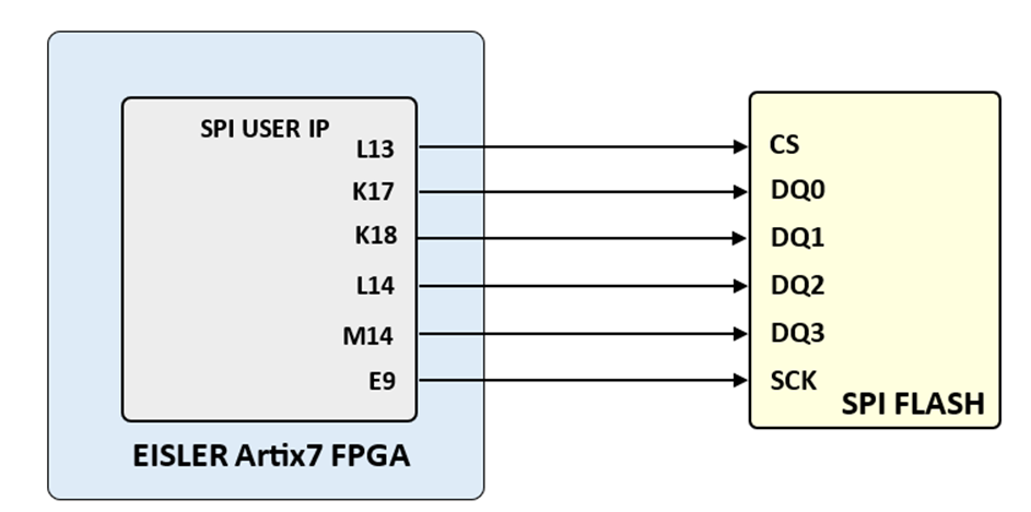
EISLER ARTIX7 FPGA BOARD ARTIX7 FPGA A7 have been loaded with a Flash device from Maronix (part number MX25L3233FM1I-08G).FPGA configuration files can be written to the Quad SPI Flash, and mode settings are available to cause the FPGA to automatically read a configuration from this device at power on. An FPGA configuration file requires just over one Mbytes of memory, leaving approximately 98% of the flash device available for user data.
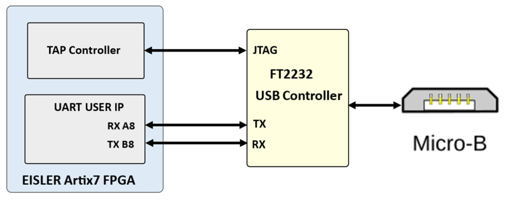
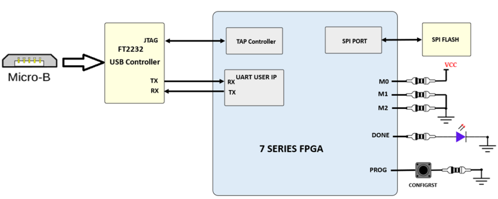
The EISLER ARTIX7 FPGA BOARD ARTIX7 FPGA A7 includes an FTDI FT2232HL
http://www.ftdichip.com/Support/Documents/DataSheets/ICs/DS_FT2232H.pdf USB-UART bridge (attached to connector J6) that allows you to use PC applications to communicate with the board using standard Windows COM port commands. Free USB-COM port drivers, available from www.ftdichip.com under the “Virtual Com Port” or VCP heading, convert USB packets to UART/serial port data. Serial port data is exchanged with the FPGA using a two-wire serial port (TXD/RXD). After the drivers are installed, I/O commands can be used from the PC directed to the COM port to produce serial data traffic on FPGA pins.
The FT2232HL is also used as the controller for the USB-JTAG circuitry, but the USB-UART and USB-JTAG functions behave entirely independent of one another. Programmers interested in using the UART functionality of the FT2232 within their design do not need to worry about the JTAG circuitry interfering with the UART data transfers, and vice-versa. The combination of these two features into a single device allows the EISLER ARTIX7 FPGA BOARD ARTIX7 FPGA A7 to be programmed, communicated with via UART, and powered from a computer attached with a single Micro USB cable. The connections between the FT2232L and the Artix-7 are shown in the below figure.
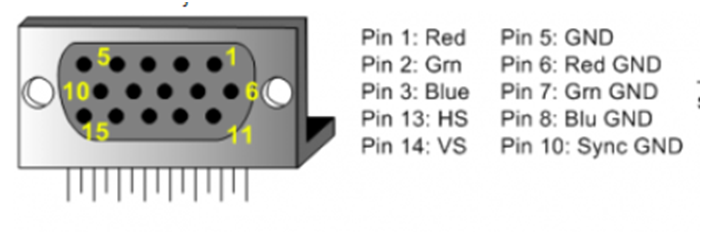
The EISLER ARTIX7 FPGA board uses 5 FPGA signals to create a VGA port with 1 bits-per-color and the two standard sync signals (HS – Horizontal Sync, and VS – Vertical Sync). The color signals use resistor-divider circuits that work in conjunction with the 82-ohm termination resistance of the VGA display to create 16 signal levels each on the red, green, and blue VGA signals.
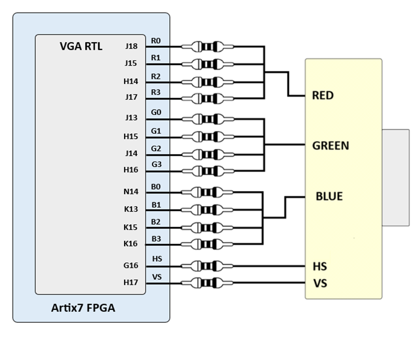
This circuit, shown in the above diagram, , produces video color signals that proceed in equal increments between 0V (fully off) and 0.7V (fully on). Using this circuit, 4096 different colors can be displayed, one for each unique 3-bit pattern. A video controller circuit must be created in the FPGA to drive the sync and color signals with the correct timing in order to produce a working display system.
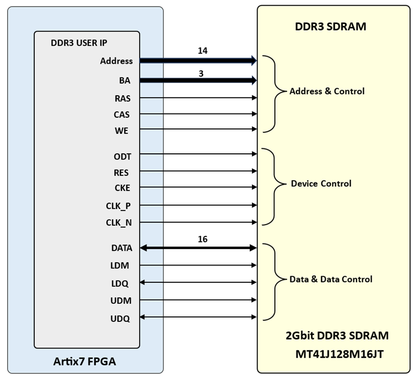
The EISLER Board includes one MT41J128M16JT-125 memory component, creating a single rank, 16-bit wide interface. It is routed to a 1.5V-powered HR (High Range) FPGA bank with 50 ohm controlled single-ended trace impedance. 50 ohm internal terminations in the FPGA are used to match the trace characteristics. Similarly, on the memory side, on-die terminations (ODT) are used for impedance matching.
For proper operation of the memory, a memory controller and physical layer (PHY) interface needs to be included in the FPGA design. The easiest way to accomplish this on the EISLER ARTIX7 FPGA BOARD ARTIX7 FPGA A7 board is to use the Xilinx 7-series memory interface solutions core generated by the MIG (Memory Interface Generator) Wizard. Depending on the tool used (ISE, EDK or Vivado), the MIG Wizard can generate a native FIFO-style or an AXI4 interface to connect to user logic. This workflow allows the customization of several DDR parameters optimized for the particular application.
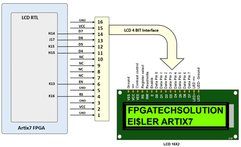
The EISLER ARTIX7 FPGAboard includes LCD16BY2 can be connected as show in following fig. LCD16BY2 is connected with 4bit interface mode
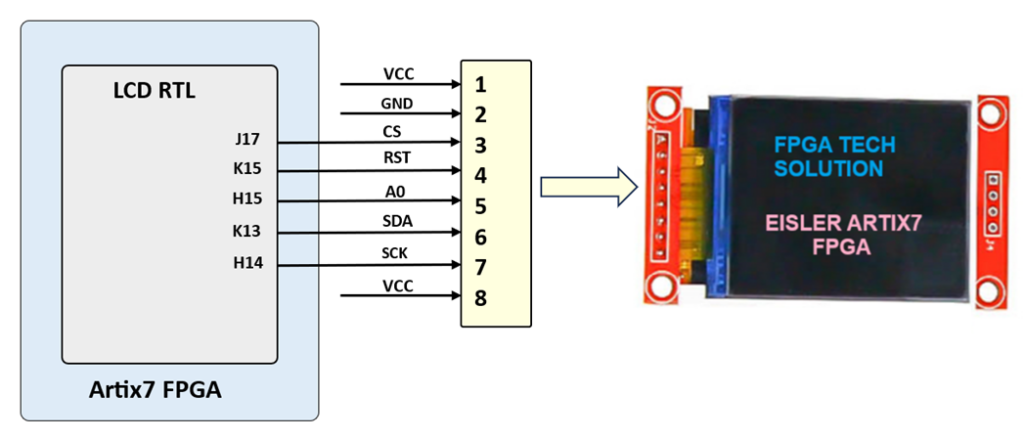
Note: Either TFT LCD or 16BY2 LCD can be used at a time
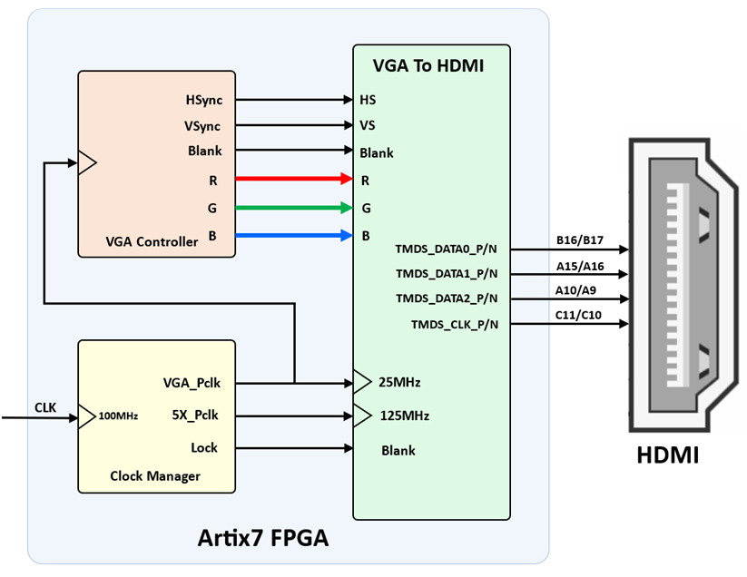
To interface an FPGA with HDMI, you need to understand both the FPGA architecture and the HDMI standard. HDMI transmits high-quality digital video and creating a proper interface involves generating the correct signals and protocols on the FPGA side.
Key Components of an FPGA HDMI Interface:
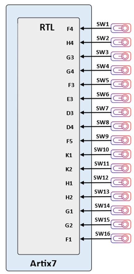
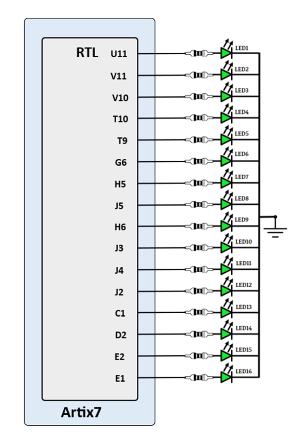
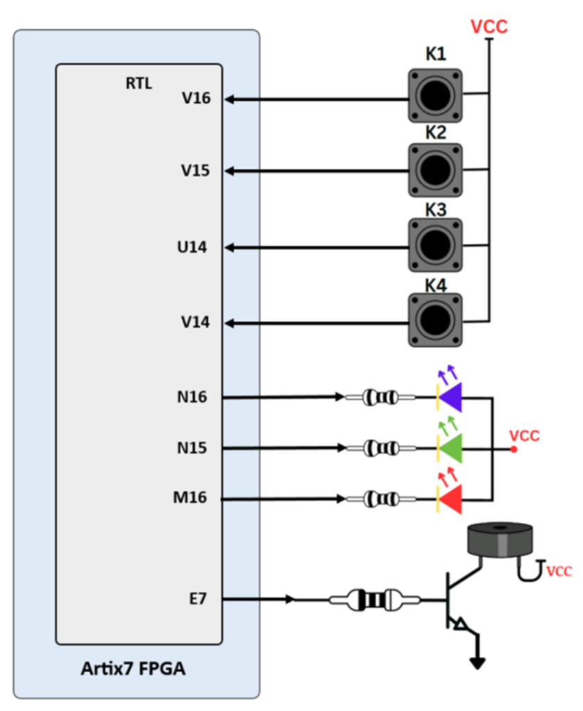
The EISLER ARTIX7 FPGA BOARD ARTIX7 FPGA A7board includes sixteen slide switches, four push buttons, sixteen individual LEDs, and a four-digit seven-segment display, as shown in the below diagram. The pushbuttons and slide switches are connected to the FPGA via series resistors to prevent damage from inadvertent short circuits (a short circuit could occur if an FPGA pin assigned to a pushbutton or slide switch was inadvertently defined as an output). The four pushbuttons are “momentary” switches that normally generate a high output when they are at rest, and a low output only when they are pressed. Slide switches generate constant high or low inputs depending on their position.
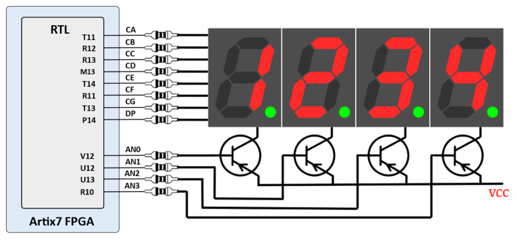
The EISLER ARTIX7 FPGAboard includes 4 common Anode seven segment display as show in following fig.
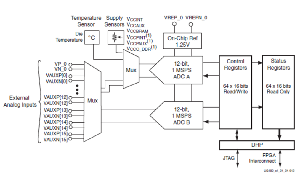
The Artix 7 FPGA chip used on the EISLER FPGA board is designed with the user in mind to provide high volume processing power for a relatively low cost. It has many powerful features including an on-board Analog-to-Digital converter (ADC) called the “XADC” available on 7 series FPGA devices provided by Xilinix. It is a dual 12-bit, 1 Mega sample per second (MSPS) ADC used to accommodate sampling for up to 17 auxiliary signals as well as including on-chip sensors for temperature and power monitoring.
The XADC supports a wide range of operating modes such as single channel, sequenced channel, duel ADC simultaneous sequence, or one-pass sequence channel sampling; event driven or continuous sampling operation; unipolar, differential, or bipolar signal sampling; etc… The XADC can also be configured to power down its individual ADCs, rearrange the order of sampling when running in a sequenced channel operation, enable averaging of samples to reduce noise, set alarms for user defined voltage and temperature tolerance violations for on-chip sensors, etc… The image below shows the block diagram of the XADC as found in the datasheet for the device as provided by Xilinix. You can download the datasheets for the XADC by clinking on the button below.
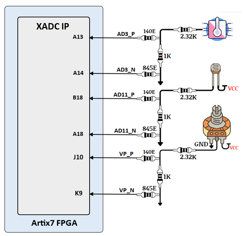
On EISLER FPGA board temperature sensor is connected with AD3_P/AD3_N channel, LDR(light dependent resistor ) is connected with AD11_P/AD11_N channel and variable resistor (POT) is connected with VP_P/VP_N channel of artix7 FPGA is shown in following fig.
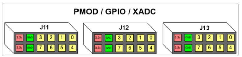
We have a large collection of Pmod (Peripheral Module) accessory boards that can attach to the expansion ports to add ready-made functions such as A/D’s, D/A’s, motor drivers, sensors, displays, and many other functions. These ports can be used as simple expansion ports, since all of the pin-outs correspond to pins on the FPGA.
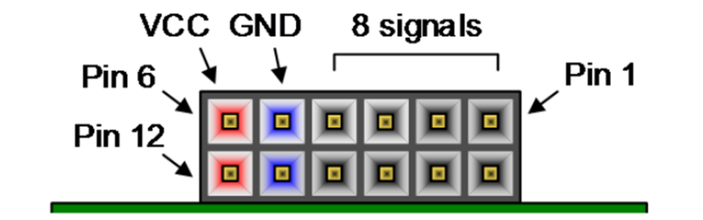
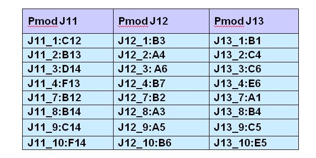
The Pmod ports are arranged in a 2×6 right-angle, and are 100-mil female connectors that mate with standard 2×6 pin headers. Each 12-pin Pmod ports provides two 3.3V VCC signals (pins 6 and 12), two Ground signals (pins 5 and 11), and eight logic signals. The VCC and Ground pins can deliver up to 1A of current. Pmod data signals are not matched pairs, and they are routed using best-available tracks without impedance control or delay matching. Pin assignments for the Pmod I/O connected to the FPGA are shown in the below table
Warning: Since the Pmod pins are connected to Artix-7FPGA pins using a 3.3V logic standard, care should be taken not to drive these pins over 3.4V.
After power-on, the FPGA must be configured (or programmed) before it can perform any functions. You can configure the FPGA in one of the following ways:
Above fig shows the different options available for configuring the FPGA. By default,on power on FPGA will be programmed by the Quad-SPI flash if it’s programed with correct .bin file.
Bitstreams are stored in volatile memory cells within the FPGA. This data defines the FPGA’s logic functions and circuit connections, and it remains valid until it is erased by removing board power, by pressing the reset button attached to the PROG input, or by writing a new configuration file using the JTAG port.
After being successfully programmed, the FPGA will cause the “DONE” LED to illuminate. Pressing the “PROG” button at any time will reset the configuration memory in the FPGA. After being reset, the FPGA will immediately attempt to reprogram itself from SPI flash, as we have fixed master spi mode.
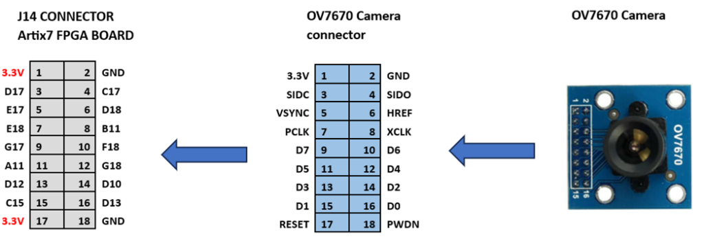
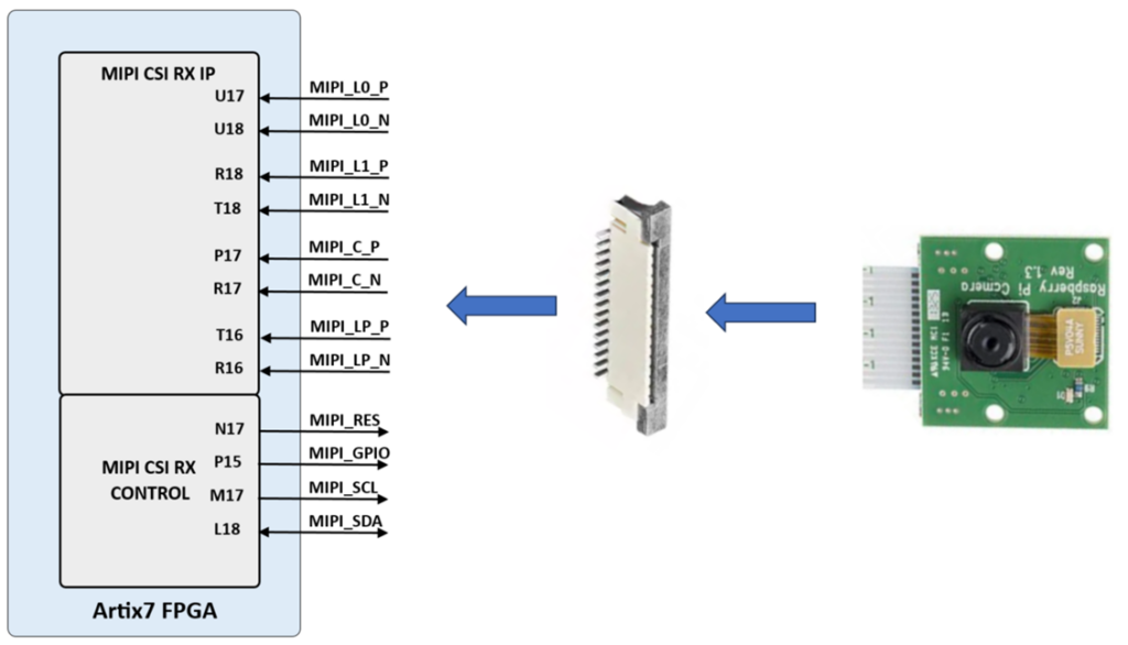
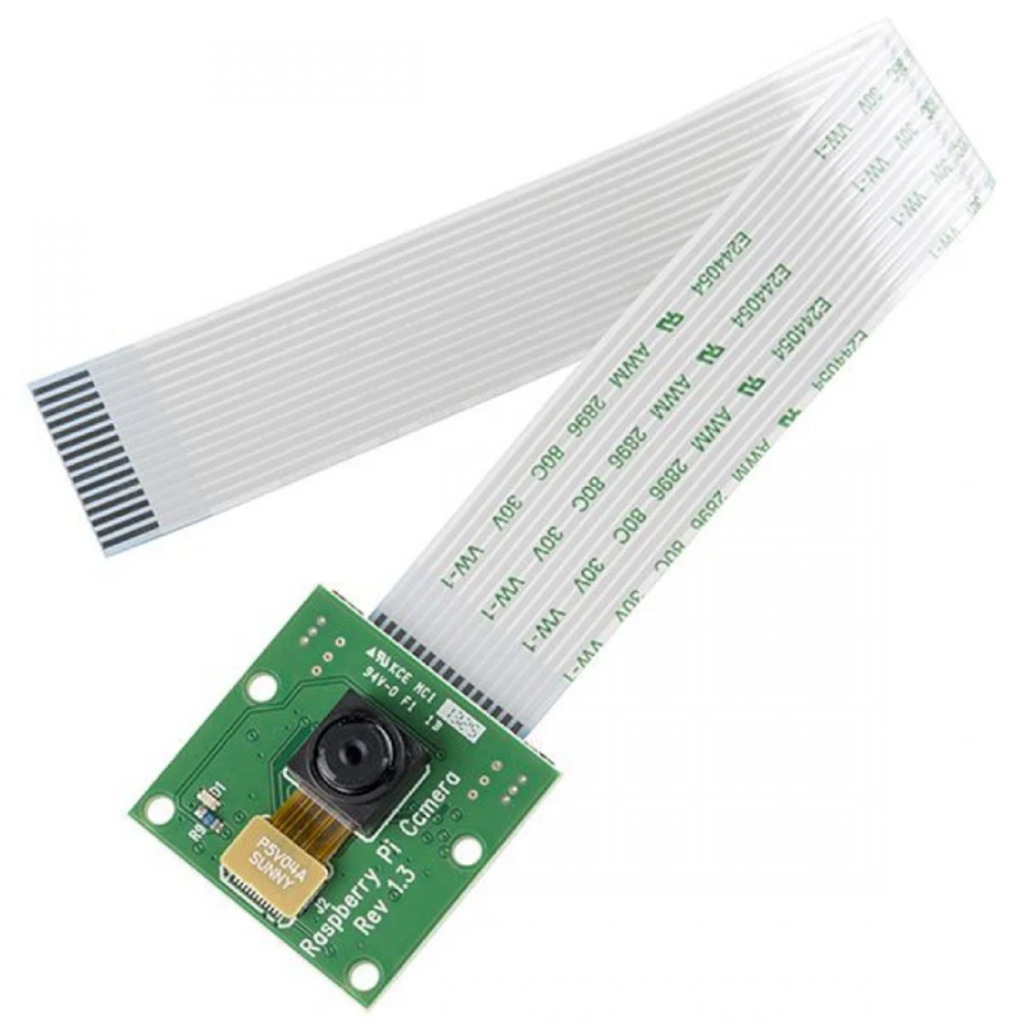
To install a camera module, connect its flex ribbon cable into the camera connector. Follow these steps:
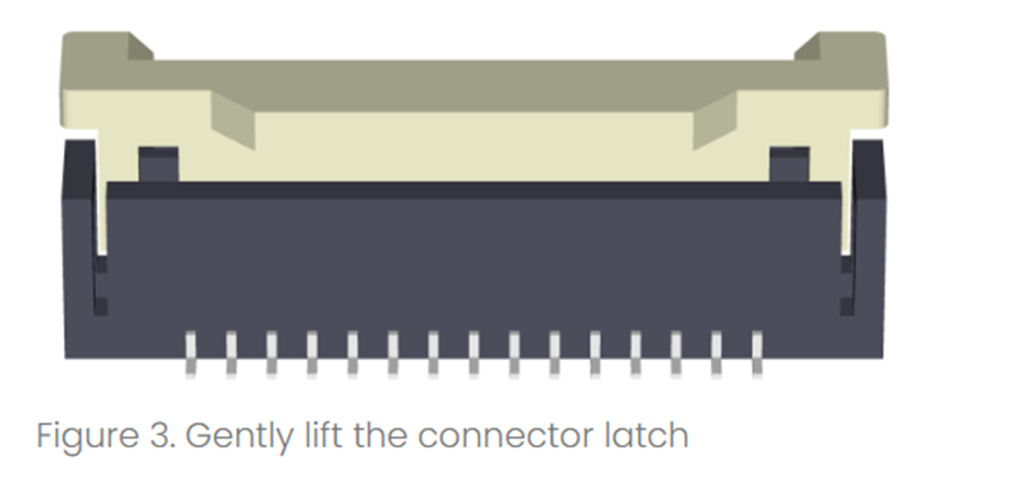
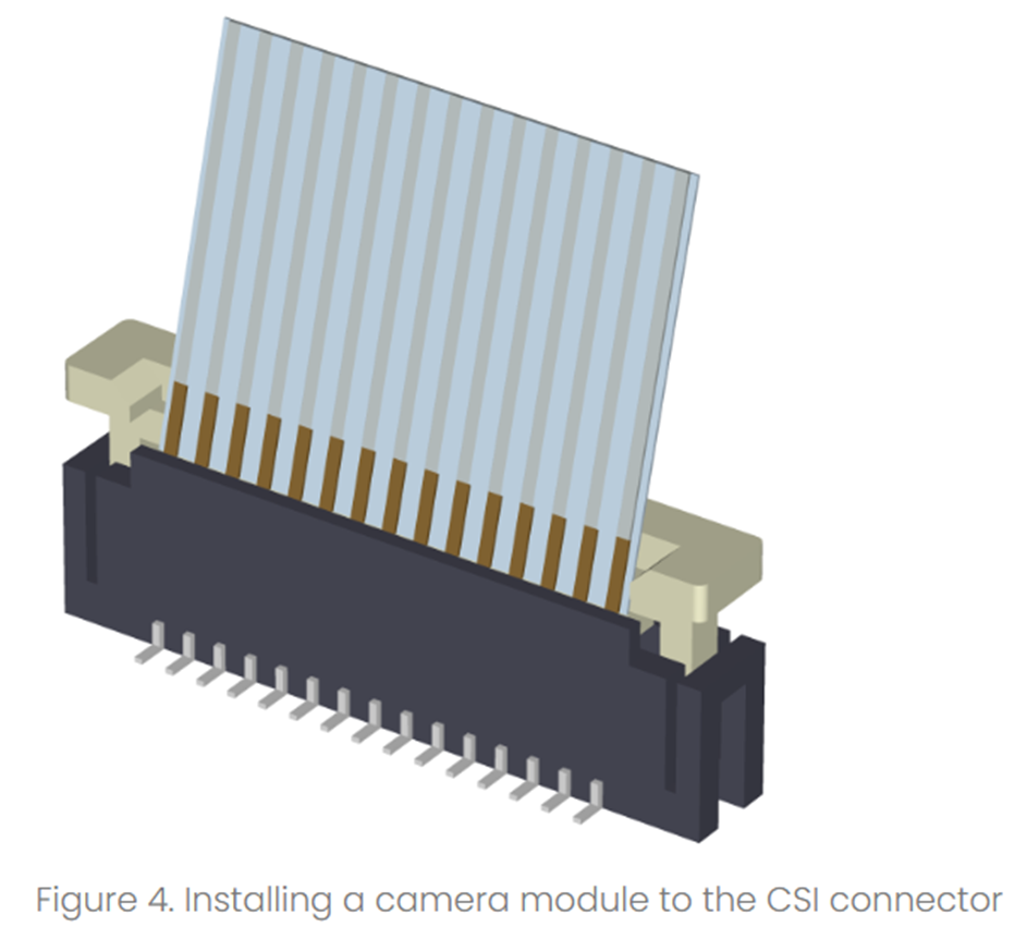
Table of Contents
Toggle