
The NETZINKY SOC board is a complete, ready-to-use digital circuit development platform based on the latest Artix7 Field Programmable Gate Array (FPGA) from Xilinx. With its high-capacity, low overall cost, and collection of USB, VGA, and other ports, the NETZINKY SOC can host designs ranging from introductory combinational circuits to complex sequential circuits like embedded processors and controllers. It includes enough switches, LEDs and other I/O devices to allow a large number designs to be completed without the need for any additional hardware, and enough uncommitted FPGA I/O pins to allow designs to be expanded using Pmods or other custom boards and circuits.
The NETZINKY SOC board has on board USB JTAG which support Vivado & vitis.
No need to purchases license, works 100% fine with webpack license
NETZINKY SoC board can be available with following part number
XC7Z020-2CLG400I
XC7Z007-1CLG400I
XC7Z010-2CLG400I
The NETZINKY works with Xilinx’s new high-performance Vivado ® Design Suite. Vivado includes many new tools and design flows that facilitate and enhance the latest design methods. It runs faster, allows better use of FPGA resources, and allows designers to focus their time evaluating design alternatives. The System Edition includes an on-chip logic analyzer, high-level synthesis tool, and other cutting-edge tools, and the free “WebPACK” version allows NETZINKY board designs to be created at no additional cost.
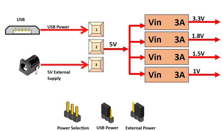
The NETZINKY Zynq7000 SoC board uses +5V power supply to function properly. By default the board is configured to use +5V supply from USB. So an external +5V power is not required unless USB port is unable to supply enough current. In most cases USB ports are capable of providing enough current for the module. Current requirement for this board largely depends on your application. Please consult Zynq7000 data sheet for more details on power requirements. If for any reason, an external 5V power supply needs to be used for the module, the Power select jumper should be configured properly as shown below When JP1 jumper is placed towards USB as shown in below image power is used from USB connector & when JP1 jumper is placed towards power connector power is used from external connector
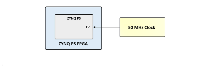
NetZinky provides a 50 MHz clock to the Zynq PS_CLK input, which is used to generate the clocks for each of the PS subsystems. The 50 MHz input allows the processor to operate at a maximum frequency of 650 MHz and the DDR3 memory controller to operate at a maximum of 525 MHz (1050 Mbps). The NetZinky Base System Design configures the PS to work properly with this input clock, and should be used as a reference when creating custom designs.
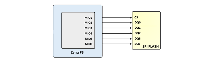
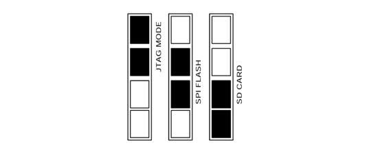
The NETZINKY features a 4-bit SPI (quad-SPI) serial NOR flash. The Spansion S25FL128S is used on this board. The Multi-I/O SPI Flash memory is used to provide non-volatile code and data storage. It can be used to initialize the PS subsystem as well as configure the PL subsystem (bitstream). Winbond Flash File System (FFS) for use after booting the Zynq-7000 AP SoC.
The SPI Flash connects to the Zynq-7000 AP SoC supporting up to Quad-I/O SPI interface. This requires connection to specific pins in MIO Bank 0/500, specifically MIO[1:6,8] as outlined in the Zynq datasheet. Quad-SPI feedback mode is used, thus qspi_sclk_fb_out/MIO[8] is left to freely toggle and is connected only to a 20K pull-up resistor to 3.3V. This allows a QSPI clock frequency greater than FQSPICLK2.
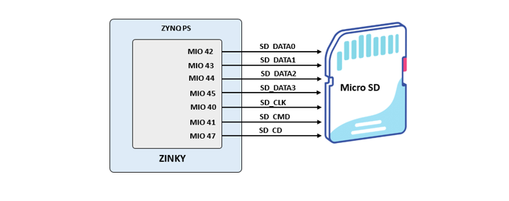
Netzinky provides a microSD slot (J14) for non-volatile external memory storage as well as booting the Zynq. The slot is wired to Bank 1/501 MIO[40-47], including Card Detect. On the PS side peripheral SDIO 0 is mapped out to these pins and controls communication with the SD card. The pinout can be seen in Table 4. The peripheral controller supports 1-bit and 4-bit SD transfer modes, but does not support SPI mode. Based on the Zynq TRM, SDIO host mode is the only mode supported.
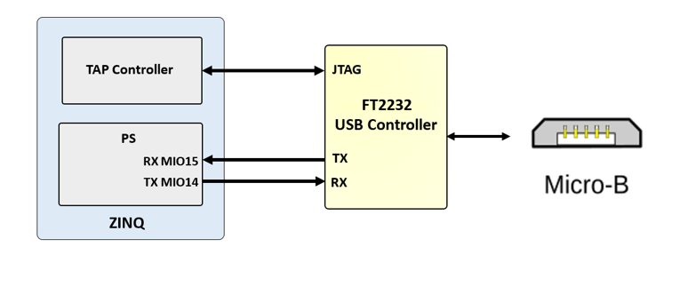
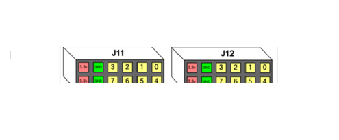
The NETZINKY includes an FTDI FT2232HQ USB-UART bridge (attached to connector J11) that lets you use PC applications to communicate with the board using standard Windows COM port commands. Free USB-COM port drivers, available from www.ftdichip.com under the “Virtual Com Port” or VCP heading, convert USB packets to UART/serial port data. Serial port data is exchanged with the Zynq using a two-wire serial port (TXD/RXD). After the drivers are installed, I/O commands can be used from the PC directed to the COM port to produce serial data traffic on the Zynq pins. The port is tied to PS (MIO) pins and can be used in combination with the UART 1 controller.
The FT2232HQ is also used as the controller for the USB-JTAG circuitry, but the USB-UART and USB-JTAG functions behave entirely independent of one another. Programmers interested in using the UART functionality of the FT2232 within their design do not need to worry about the JTAG circuitry interfering with the UART data transfers, and vice-versa. The combination of these two features into a single device allows the NETZINKY to be programmed, communicated with via UART, and powered from a computer attached with a single Micro USB cable.
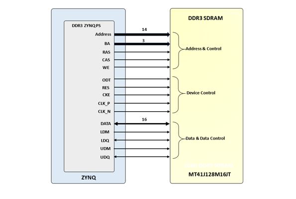
The NETZINKY Board includes one MT41J128M16JT-125 memory component, creating a single rank, 16-bit wide interface. It is routed to a 1.5V-powered HR (High Range) FPGA bank with 50 ohm controlled single-ended trace impedance. 50 ohm internal terminations in the FPGA are used to match the trace characteristics. Similarly, on the memory side, on-die terminations (ODT) are used for impedance matching.
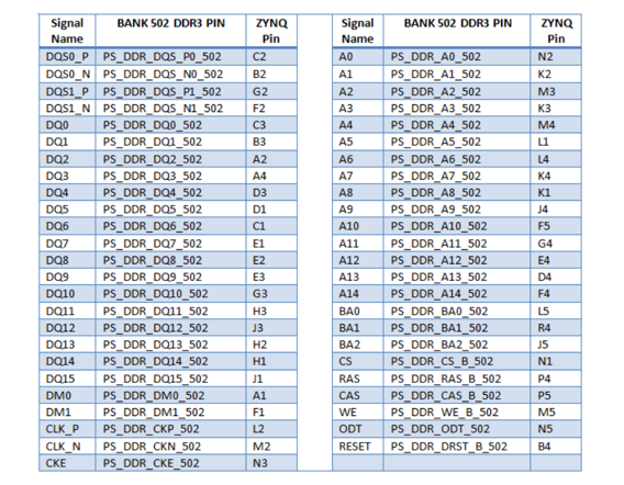
The DDR3 memory system is directly connected to the memory interface of the BANK 502 of the ZYNQ processing system (PS).Both the memory chips and the PS DDR bank are powered from the 1.5V supply. The mid-point reference of 0.75V is created with a simple resistor divider and is available to the Zynq as external reference.
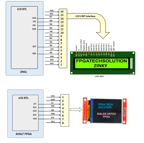
The NETZINKY FPGA board includes LCD16BY2 can be connected as show in following fig. LCD16BY2 is connected with 4bit interface mode
Note: Either TFT LCD or 16BY2 LCD can be used at a time
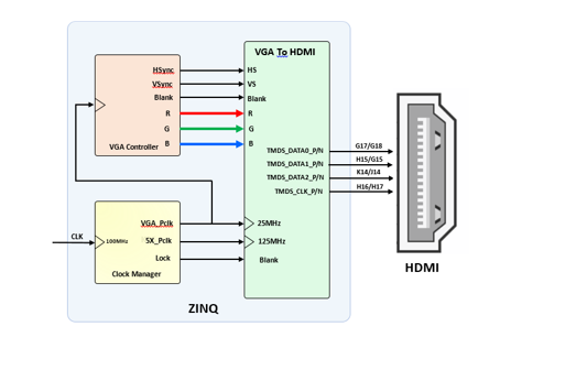
To interface an FPGA with HDMI, you need to understand both the FPGA architecture and the HDMI standard. HDMI transmits high-quality digital video and creating a proper interface involves generating the correct signals and protocols on the FPGA side.
Key Components of an FPGA HDMI Interface:
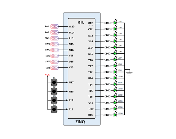
The NETZINKY SOCboard includes sixteen slide switches, four push buttons, sixteen individual LEDs, and a four-digit seven-segment display, as shown in the below diagram. The pushbuttons and slide switches are connected to the FPGA via series resistors to prevent damage from inadvertent short circuits (a short circuit could occur if an FPGA pin assigned to a pushbutton or slide switch was inadvertently defined as an output). The four pushbuttons are “momentary” switches that normally generate a high output when they are at rest, and a low output only when they are pressed. Slide switches generate constant high or low inputs depending on their position.
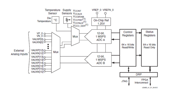
The Artix 7 FPGA chip used on the NETZINKY FPGA board is designed with the user in mind to provide high volume processing power for a relatively low cost. It has many powerful features including an on-board Analog-to-Digital converter (ADC) called the “XADC” available on 7 series FPGA devices provided by Xilinix. It is a dual 12-bit, 1 Mega sample per second (MSPS) ADC used to accommodate sampling for up to 17 auxiliary signals as well as including on-chip sensors for temperature and power monitoring.
The XADC supports a wide range of operating modes such as single channel, sequenced channel, duel ADC simultaneous sequence, or one-pass sequence channel sampling; event driven or continuous sampling operation; unipolar, differential, or bipolar signal sampling; etc… The XADC can also be configured to power down its individual ADCs, rearrange the order of sampling when running in a sequenced channel operation, enable averaging of samples to reduce noise, set alarms for user defined voltage and temperature tolerance violations for on-chip sensors, etc… The image below shows the block diagram of the XADC as found in the datasheet for the device as provided by Xilinix. You can download the datasheets for the XADC by clinking on the button below.
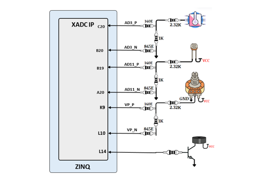
On NETZINKY board temperature sensor is connected with AD3_P/AD3_N channel, LDR(light dependent resistor ) is connected with AD11_P/AD11_N channel and variable resistor (POT) is connected with VP_P/VP_N channel of artix7 FPGA is shown in following fig.
The NETZINKY FPGA board includes 4 common Anode seven segment display as show in following fig.
We have a large collection of Pmod (Peripheral Module) accessory boards that can attach to the expansion ports to add ready-made functions such as A/D’s, D/A’s, motor drivers, sensors, displays, and many other functions. These ports can be used as simple expansion ports, since all of the pin-outs correspond to pins on the FPGA.
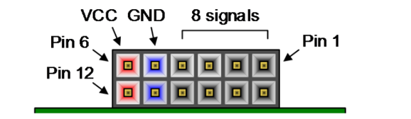
The Pmod ports are arranged in a 2×6 right-angle, and are 100-mil female connectors that mate with standard 2×6 pin headers. Each 12-pin Pmod ports provides two 3.3V VCC signals (pins 6 and 12), two Ground signals (pins 5 and 11), and eight logic signals. The VCC and Ground pins can deliver up to 1A of current. Pmod data signals are not matched pairs, and they are routed using best-available tracks without impedance control or delay matching. Pin assignments for the Pmod I/O connected to the FPGA are shown in the below table
Warning: Since the Pmod pins are connected to Artix-7FPGA pins using a 3.3V logic standard, care should be taken not to drive these pins over 3.4V.
Unlike Xilinx FPGA devices, AP SoC devices such as the Zynq-7010 are designed around the processor, which acts as a master to the programmable logic fabric and all other on-chip peripherals in the processing system. This causes the Zynq boot process to be more similar to that of a microcontroller than an FPGA. This process involves the processor loading and executing a Zynq Boot Image, which includes a First Stage Bootloader (FSBL), a bitstream for configuring the programmable logic (optional), and a user application. The boot process is broken into three stages:
J3 connector will select configuration mode
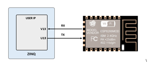
Netzinky has a ESP8266 wifi, connection as follows
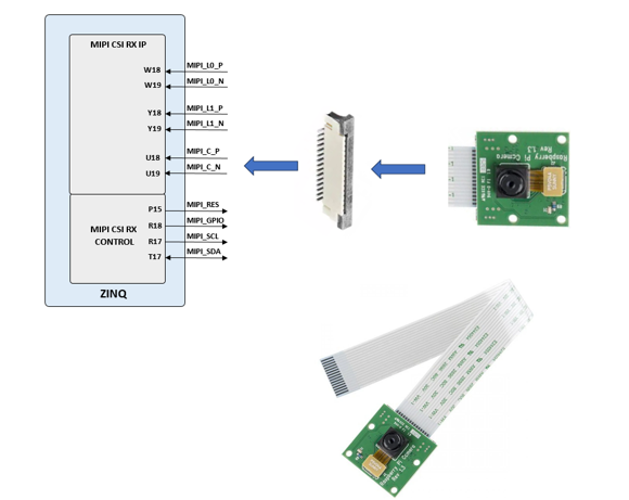
To install a camera module, connect its flex ribbon cable into the camera connector. Follow these steps:
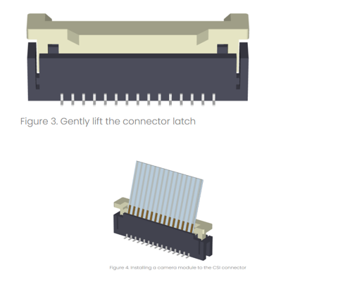
To install a camera module, connect its flex ribbon cable into the camera connector. Follow these steps:
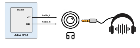
Table of Contents
Toggle