
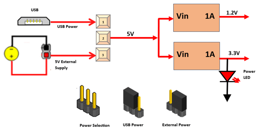
TheMINI-SP6-FPGAboard can work on USB power; you can also connect external 5VDC supply. When JP2 jumper is placed towards USB as shown in below imagepower is used from USB connector & when JP2 jumper is placed towards EXT power is used from J4 connector(J4 is optional)
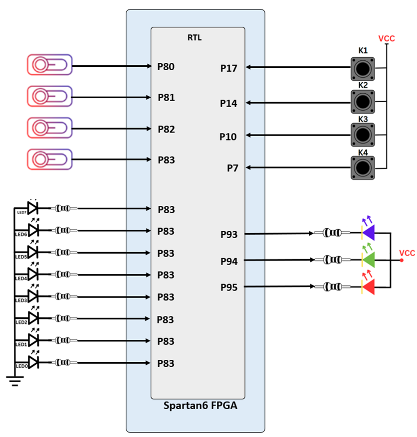
The Spartan6-Mini board includes 4dip switches, four push buttons, eight individual LEDs, and a RGB LED, as shown in the below diagram. The pushbuttons and slide switches are connected to the FPGA via series resistors to prevent damage from inadvertent short circuits (a short circuit could occur if an FPGA pin assigned to a pushbutton or slide switch was inadvertently defined as an output). The four pushbuttons are “momentary” switches that normally generate a high output when they are at rest, and a High output only when they are pressed. Slide switches generate constant high or low inputs depending on their position.
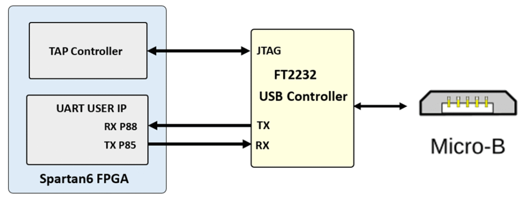
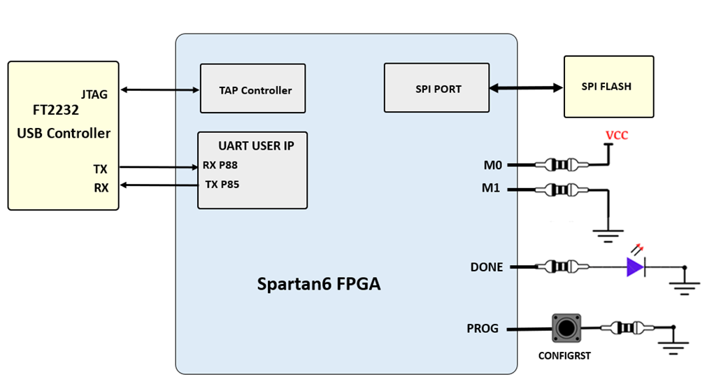
http://www.ftdichip.com/Support/Documents/DataSheets/ICs/DS_FT2232H.pdf USB-UART bridge (attached to connector J6) that allows you to use PC applications to communicate with the board using standard Windows COM port commands. Free USB-COM port drivers, available from www.ftdichip.com under the “Virtual Com Port” or VCP heading, convert USB packets to UART/serial port data. Serial port data is exchanged with the FPGA using a two-wire serial port (TXD/RXD). After the drivers are installed, I/O commands can be used from the PC directed to the COM port to produce serial data traffic on FPGA pins.
The FT2232HL is also used as the controller for the USB-JTAG circuitry, but the USB-UART and USB-JTAG functions behave entirely independent of one another. Programmers interested in using the UART functionality of the FT2232 within their design do not need to worry about the JTAG circuitry interfering with the UART data transfers, and vice-versa. The combination of these two features into a single device allows the Spartan6-Mini to be programmed, communicated with via UART, and powered from a computer attached with a single Micro USB cable. The connections between the FT2232L and the Spartan6 are shown in the below figure.
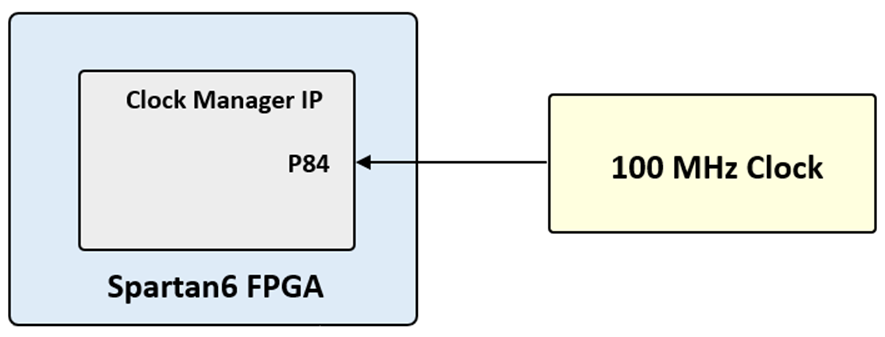
The Spartan6-Mini includes a single 100MHz oscillator connected to pin P84 can drive MMCMs or PLLs to generate clocks of various frequencies and with known phase relationships that may be needed throughout a design. Some rules restrict which MMCMs and PLLs may be driven by the 100MHz input clock. For a full description of these rules and of the capabilities of the Spartan6 clocking resources
Xilinx offers the Clocking Wizard IP core to help users generate the different clocks required for a specific design. This wizard properly instantiates the needed MMCMs and PLLs based on the desired frequencies and phase relationships specified by the user. The wizard will then output an easy to use wrapper component around these clocking resources that can be inserted into the user’s design.
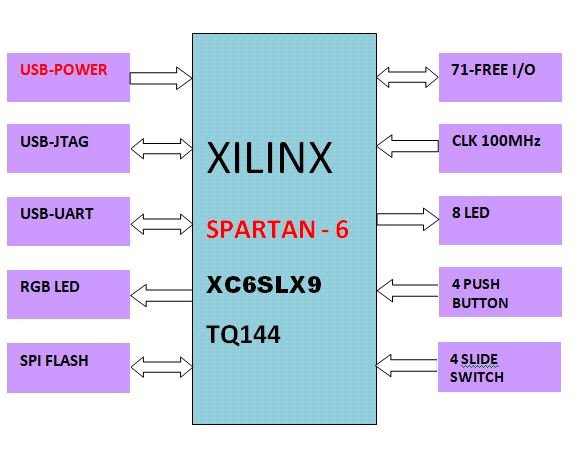
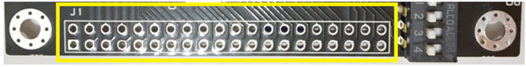
The MINI-SP6-FPGA-V1 board has total 71 user I/O placedtwo input output connectors. J1 connector has 35 input output pins. J2 connector has 36 input output pins.
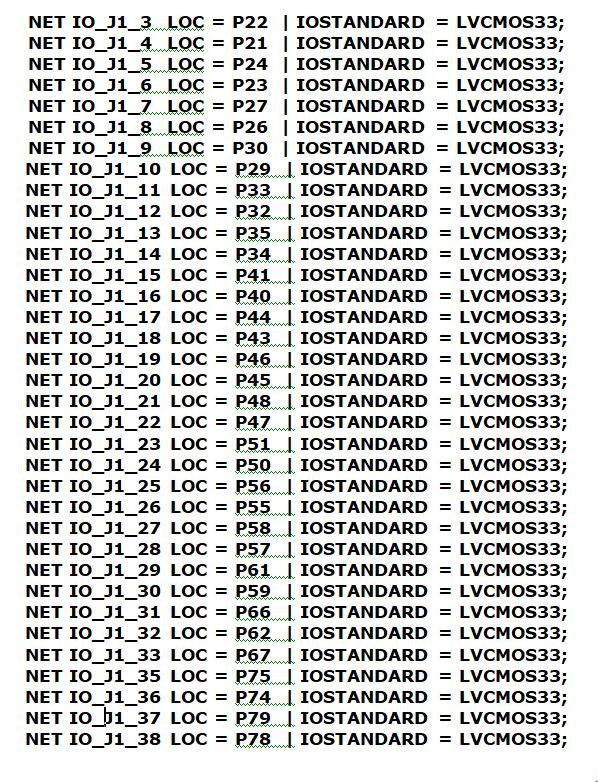
All pin can work with maximum 3.3V DC
| Name | Signal Name | XCS6LX9-TQG144 |
|---|---|---|
| J1 | J1_1 | GND |
| J1 | J1_3 | P22 |
| J1 | J1_5 | P24 |
| J1 | J1_7 | P27 |
| J1 | J1_9 | P30 |
| J1 | J1_11 | P33 |
| J1 | J1_13 | P35 |
| J1 | J1_15 | P41 |
| J1 | J1_17 | P44 |
| J1 | J1_19 | P46 |
| J1 | J1_21 | P48 |
| J1 | J1_23 | P51 |
| J1 | J1_25 | P56 |
| J1 | J1_27 | P58 |
| J1 | J1_29 | P61 |
| J1 | J1_31 | P66 |
| J1 | J1_33 | P67 |
| J1 | J1_35 | P75 |
| J1 | J1_37 | P79 |
| J1 | J1_39 | +3.3V |
| Name | Signal Name | XCS6LX9-TQG144 |
|---|---|---|
| J1 | J1_2 | GND |
| J1 | J1_4 | P21 |
| J1 | J1_6 | P23 |
| J1 | J1_8 | P26 |
| J1 | J1_10 | P29 |
| J1 | J1_12 | P32 |
| J1 | J1_14 | P34 |
| J1 | J1_16 | P40 |
| J1 | J1_18 | P43 |
| J1 | J1_20 | P45 |
| J1 | J1_22 | P47 |
| J1 | J1_24 | P50 |
| J1 | J1_26 | P55 |
| J1 | J1_28 | P57 |
| J1 | J1_30 | P59 |
| J1 | J1_32 | P62 |
| J1 | J1_34 | NC |
| J1 | J1_36 | P74 |
| J1 | J1_38 | P78 |
| J1 | J1_40 | +3.3V |
| Name | Signal Name | XCS6LX9-TQG144 |
|---|---|---|
| J2 | J2_1 | GND |
| J2 | J2_3 | P1 |
| J2 | J2_5 | P143 |
| J2 | J2_7 | P141 |
| J2 | J2_9 | P139 |
| J2 | J2_11 | P137 |
| J2 | J2_13 | P13 |
| J2 | J2_15 | P131 |
| J2 | J2_17 | P126 |
| J2 | J2_19 | P123 |
| J2 | J2_21 | P120 |
| J2 | J2_23 | P118 |
| J2 | J2_25 | P116 |
| J2 | J2_27 | P114 |
| J2 | J2_29 | P111 |
| J2 | J2_31 | P104 |
| J2 | J2_33 | P101 |
| J2 | J2_35 | P99 |
| J2 | J2_37 | P97 |
| J2 | J2_39 | +3.3V |
| Name | Signal Name | XCS6LX9-TQG144 |
|---|---|---|
| J2 | J2_2 | GND |
| J2 | J2_4 | P2 |
| J2 | J2_6 | P144 |
| J2 | J2_8 | P142 |
| J2 | J2_10 | P140 |
| J2 | J2_12 | P138 |
| J2 | J2_14 | P134 |
| J2 | J2_16 | P132 |
| J2 | J2_18 | P127 |
| J2 | J2_20 | P124 |
| J2 | J2_22 | P121 |
| J2 | J2_24 | P119 |
| J2 | J2_26 | P117 |
| J2 | J2_28 | P115 |
| J2 | J2_30 | P112 |
| J2 | J2_32 | P105 |
| J2 | J2_34 | P102 |
| J2 | J2_36 | P100 |
| J2 | J2_38 | P97 |
| J2 | J2_40 | +3.3V |
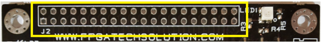
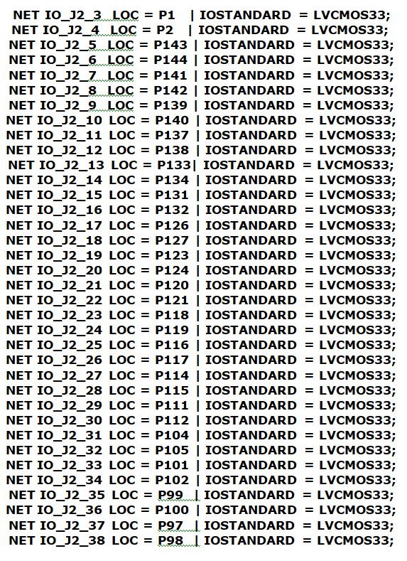
Table of Contents
Toggle