
The ZINKY SOC board is a complete, ready-to-use digital circuit development platform based on the latest Artix7 Field Programmable Gate Array (FPGA) from Xilinx. With its high-capacity, low overall cost, and collection of USB, HDMI, and other ports, the ZINKY SOC can host designs ranging from introductory combinational circuits to complex sequential circuits like embedded processors and controllers. It includes 120+ uncommitted FPGA I/O pins to allow designs to be expanded using burg or other custom boards and circuits.
The ZINKY SOC board has on board USB JTAG which support Vivado & vitis.
No need to purchases license, works 100% fine with webpack license
ZINKY SoC board can be available with following part number
XC7Z020-2CLG400I
XC7Z007-1CLG400I
XC7Z010-2CLG400I
The ZINKY works with Xilinx’s new high-performance Vivado ® Design Suite. Vivado includes many new tools and design flows that facilitate and enhance the latest design methods. It runs faster, allows better use of FPGA resources, and allows designers to focus their time evaluating design alternatives. The System Edition includes an on-chip logic analyzer, high-level synthesis tool, and other cutting-edge tools, and the free “WebPACK” version allows ZINKY board designs to be created at no additional cost.
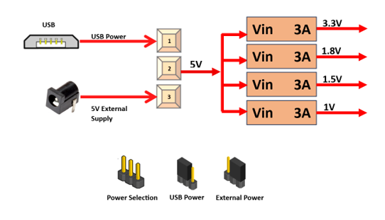
The ZINKY Zynq7000 SoC board uses +5V to 18V power supply to function properly. By default the board is configured to use +5V to 18V supply from USB. So an external +5V to 18V power is not required unless USB port is unable to supply enough current. In most cases USB ports are capable of providing enough current for the module. Current requirement for this board largely depends on your application. Please consult Zynq7000 data sheet for more details on power requirements. If for any reason, an external +5V to 18V power supply needs to be used for the module, the Power select jumper should be configured properly as shown below When JP1 jumper is placed towards USB as shown in below image power is used from USB connector & when JP1 jumper is placed towards power connector power is used from external connector
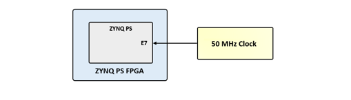
Zinky provides a 50 MHz clock to the Zynq PS_CLK input, which is used to generate the clocks for each of the PS subsystems. The 50 MHz input allows the processor to operate at a maximum frequency of 650 MHz and the DDR3 memory controller to operate at a maximum of 525 MHz (1050 Mbps). The Zinky Base System Design configures the PS to work properly with this input clock, and should be used as a reference when creating custom designs.
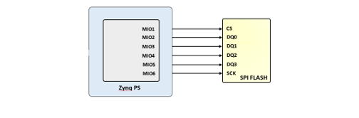
The ZINKY features a 4-bit SPI (quad-SPI) serial NOR flash. The Spansion S25FL128S is used on this board. The Multi-I/O SPI Flash memory is used to provide non-volatile code and data storage. It can be used to initialize the PS subsystem as well as configure the PL subsystem (bitstream). Winbond Flash File System (FFS) for use after booting the Zynq-7000 AP SoC.
The SPI Flash connects to the Zynq-7000 AP SoC supporting up to Quad-I/O SPI interface. This requires connection to specific pins in MIO Bank 0/500, specifically MIO[1:6,8] as outlined in the Zynq datasheet. Quad-SPI feedback mode is used, thus qspi_sclk_fb_out/MIO[8] is left to freely toggle and is connected only to a 20K pull-up resistor to 3.3V. This allows a QSPI clock frequency greater than FQSPICLK2.
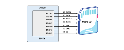
Zinky provides a microSD slot (J14) for non-volatile external memory storage as well as booting the Zynq. The slot is wired to Bank 1/501 MIO[40-47], including Card Detect. On the PS side peripheral SDIO 0 is mapped out to these pins and controls communication with the SD card. The pinout can be seen in Table 4. The peripheral controller supports 1-bit and 4-bit SD transfer modes, but does not support SPI mode. Based on the Zynq TRM, SDIO host mode is the only mode supported.
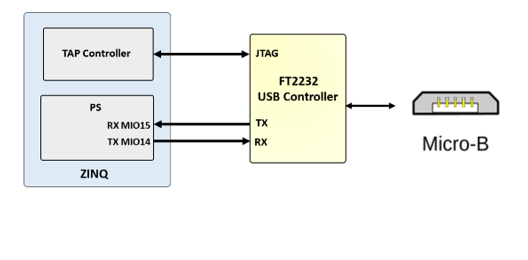
The ZINKY includes an FTDI FT2232HQ USB-UART bridge (attached to connector J11) that lets you use PC applications to communicate with the board using standard Windows COM port commands. Free USB-COM port drivers, available from www.ftdichip.com under the “Virtual Com Port” or VCP heading, convert USB packets to UART/serial port data. Serial port data is exchanged with the Zynq using a two-wire serial port (TXD/RXD). After the drivers are installed, I/O commands can be used from the PC directed to the COM port to produce serial data traffic on the Zynq pins. The port is tied to PS (MIO) pins and can be used in combination with the UART 1 controller.
The FT2232HQ is also used as the controller for the USB-JTAG circuitry, but the USB-UART and USB-JTAG functions behave entirely independent of one another. Programmers interested in using the UART functionality of the FT2232 within their design do not need to worry about the JTAG circuitry interfering with the UART data transfers, and vice-versa. The combination of these two features into a single device allows the ZINKY to be programmed, communicated with via UART, and powered from a computer attached with a single Micro USB cable.
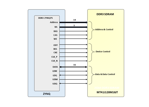
The ZINKY Board includes one MT41J128M16JT-125 memory component, creating a single rank, 16-bit wide interface. It is routed to a 1.5V-powered HR (High Range) FPGA bank with 50 ohm controlled single-ended trace impedance. 50 ohm internal terminations in the FPGA are used to match the trace characteristics. Similarly, on the memory side, on-die terminations (ODT) are used for impedance matching.
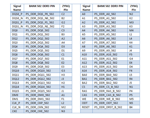
The DDR3 memory system is directly connected to the memory interface of the BANK 502 of the ZYNQ processing system (PS).Both the memory chips and the PS DDR bank are powered from the 1.5V supply. The mid-point reference of 0.75V is created with a simple resistor divider and is available to the Zynq as external reference.
Unlike Xilinx FPGA devices, AP SoC devices such as the Zynq-7020 are designed around the processor, which acts as a master to the programmable logic fabric and all other on-chip peripherals in the processing system. This causes the Zynq boot process to be more similar to that of a microcontroller than an FPGA. This process involves the processor loading and executing a Zynq Boot Image, which includes a First Stage Bootloader (FSBL), a bitstream for configuring the programmable logic (optional), and a user application. The boot process is broken into three stages:
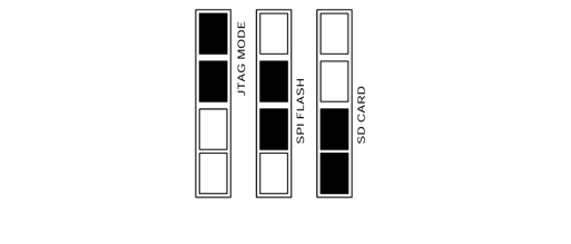
J3 connector will select configuration mode
Zynq-7020 includes 120+ uncommitted FPGA I/O pins to allow designs to be expanded using burg or other custom boards and circuits
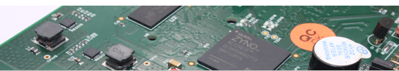
Table of Contents
Toggle